[custom_headline type=”left” level=”h1″ looks_like=”h2″]EBIC[/custom_headline]
Correlate topography, composition and structure with electrical activity.
Correlate topography, composition and structure with electrical activity.
- Record simultaneous EBIC, SE, BSE and EDS signals.
- Colour and mix signals for spatial correlation.
- Distinguish between active and passive defects.
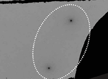
Enable TEM or atom probe microscopy sample preparation.
- Localise defects with sufficient resolution for TEM sample preparation.
- Avoid alignment error by directly imaging defects with EBIC in FIB SEM.
- Use live EBIC imaging to stop ion milling for sample preparation.
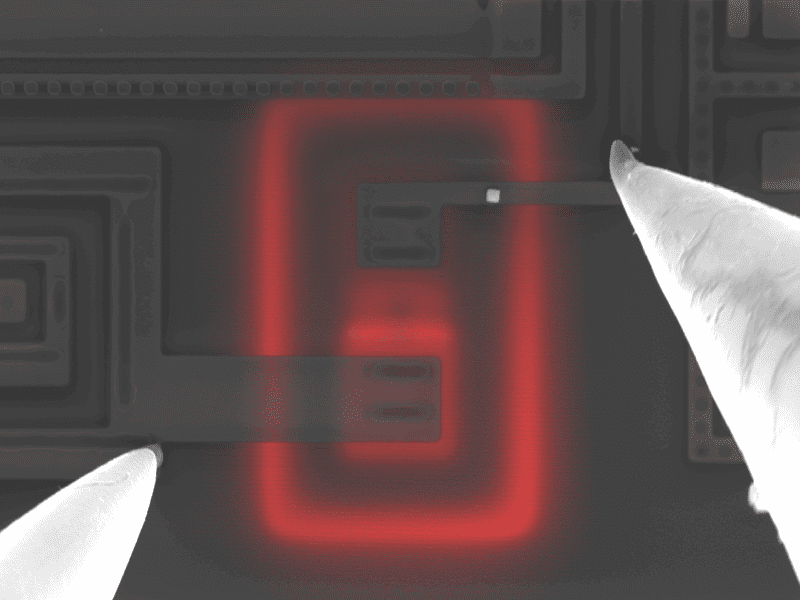
Verify device operation modes with built-in biasing and live overlay.
- Image junctions and fields in delayered operating devices.
- Map electrical activity of solar cells under bias.
- Compare imaged behaviour with device modelling.
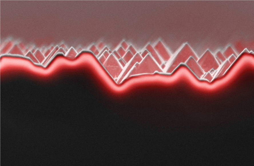
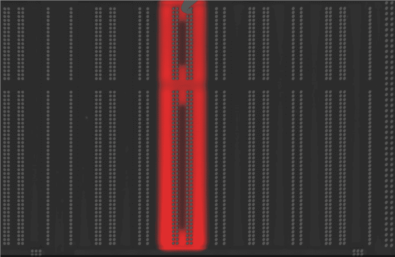
Map junctions and defects with the highest possible resolution.
- Correlate structural defects with electrical activity.
- Map active areas of junctions and electrical fields.
- Validate doping profiles and areas.
Access third dimension with depth profiling.
- Manipulate depth of EBIC signal by changing kV in SEM.
- Investigate EBIC images of cross-sections in FIB-SEM.
- Export EBIC depth series for 3D reconstruction.

