[custom_headline type=”left” level=”h1″ looks_like=”h2″]NENOVISION – LiteScope TM[/custom_headline]
Scanning Probe Microscope designed for integration into the Scanning Electron Microscopes offering unique Correlative Probe and Electron Microscopy technique.
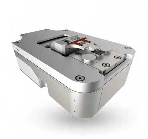
LiteScope™ is a unique Scanning Probe Microscope (SPM). It is designed for easy integration into various Scanning Electron Microscopes (SEM).
The combination of the complementary SPM and SEM techniques enables it to utilize the advantages of both.
The design of LiteScope™ also enables it to be combined with other SEM accessories such as a Focused Ion Beam (FIB) or Gas Injection System (GIS) for the fabrication of nano / microstructures and surface modifications. In this combination, LiteScope™ offers quick and easy 3D inspection of the fabricated structures.
Furthermore, LiteScope™ opens up a completely new field of novel measurement techniques which enables correlative microscopy, so-called Correlative Probe and Electron Microscopy (CPEM). The CPEM technology is the first of its kind on the market. It enables both SPM and SEM measurements to be taken in the same place, at the same time, and using the same coordination system. Only CPEM technology brings you the full advantages of the correlative imaging of the SPM and SEM techniques.
Correlative Probe and Electron Microscopy – CPEM
LiteScope™ is a powerful enhancement to how existing SEM instruments work. However, there is more to it than that.
Correlative microscopy brings together the benefits of imaging the same object using two different techniques. The correlation of the data from the separate images provides more detailed information about the sample, which would otherwise be too complicated to analyse.
NenoVision has developed unique technology – Correlative Probe and Electron Microscopy (patent pending) – for application in correlative imaging.
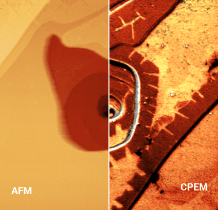
CPEM enables the determination of the surface characterization of a sample area by both SEM and SPM simultaneously and using the same coordination system.
CPEM technology enables correlative imaging of the standard SEM and SPM methods in a manner that has not been available until now.
CPEM synchronizes the scanned area, resolution and image distortion and correlates the acquired SPM and SEM images in real time.
Simultaneous scanning with known constant offset and identical resolution ensures that the analysis is performed on the same surface. The resulting image can be directly viewed on-line using our NenoView software.
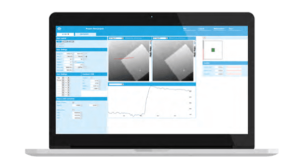
NenoView Software
NenoView software is user friendly and gives you full control of the measurement set-up, data acquisition and data processing. NenoView automatically saves the measurement setup with the data; this feature is very helpful for later analyses.
Control Unit
All the electronics that drive LiteScope™ are integrated in one control unit. This unit is a standard 19” rack mount which can easily be placed into a free slot of the SEM electronics or positioned freely according to your actual needs.
SEM Integration
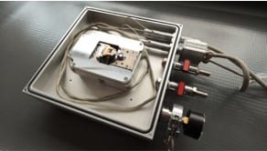
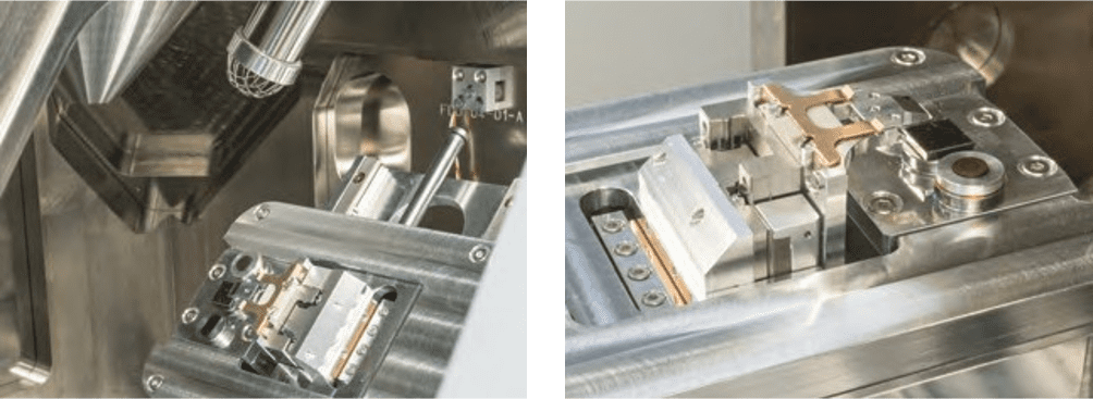
LiteScope™ is specifically designed to be integrated into SEM microscopes on a “Plug & Play” basis. LiteScope™ is simply attached to the sample stage of the electron microscope by four screws. The electrical cables are plugged into the prepared vacuum feedthrough. LiteScope™ can be mounted or removed in less than 5 minutes. LiteScope™ can be easily integrated into the electron microscopes of different manufactures. We provide the appropriate adapters and feedthroughs, which can also be adjusted according to customer needs.
Highlights
- LiteScope™ improves the performance of the SEM,
- Available as a plug-in for existing microscopes or as a new SEM,
- Unique Correlative Probe and Electron Microscopy (CPEM) technology,
- Complex surface characterization – topography, roughness, magnetic properties, conductivity, electrical properties,
- Self-sensing probes without optical detection, no laser adjustments,
- LiteScope™ is easy to mount to / remove from the sample stage of the SEM,
Application
LiteScope™ has many applications ranging from basic academic research to failure analysis
in industry. The main applications are related to analysis, in particular where conventional SEM does not provide sufficient information and additional 3D imaging is required using a SPM. The availability of other or complementary imaging modes broadens the application field even more.
The unique CPEM technology, with its correlative imaging, can be applied to highly demanding
fields where imaging using conventional SEM may provide misleading information due to surface contamination related to the chemical contrast which interferes with the surface topography. CPEM is the ideal solution for the accurate analysis and interpretation of images in real time.
Basic research in the field of material science and nanotechnology requires detailed and full analysis of surfaces and nanostructures using different analytical methods. This is based on the need to fully understand the principles of the nanoscale range. LiteScope™ is the ideal tool for these scientific applications. The immediate advantage is evident for technologies like FIB and GIS where the structures are formed directly in the SEM. The 3D analysis tool for the newly created structures is essential.
Furthermore, LiteScope™, equipped with CPEM and other imaging modes, enables the complex analysis of prepared structures and nano-devices.
In industrial quality control and R&D laboratories, LiteScope™ helps to identify surface structures, topography, surface roughness, contamination, etc. These abilities are highly prized by industrial customers who need to verify the quality of a surface and therefore save on losses due to failure.
LiteScope™ can be applied to a broad range of industries, including those in the fields of semiconductors, solar cells, memory devices, MEMS and NEMS. These fields require nanoscale analysis more than any others. Nowadays, the requirements for complex analysis of nano-circuits and nano-devices are increasing. LiteScope™ fulfils those demands by extending the 3D imaging and multi-characterization of samples in real time.
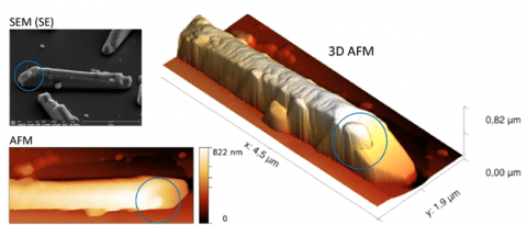
Analysis of 2D materials by AFM-in-SEM LiteScope
Load-lock mechanism for AFM-in-SEM LiteScope
NenoVision Webinar Series: Measuring tutorial with LiteScope
NenoVision Webinar Series: Advantages of combining AFM with FIB-SEM systems
NenoVision Webinar Series: Applications for 2D materials
NenoVision Webinar Series: CPEM technology – next step in correlative imaging
NenoVision Webinar Series: LiteScope overview – Merge the forces of AFM and SEM
04/02/2021 Webinar Correlative microscopy AFM in SEM
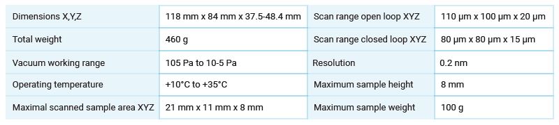
Technical Specifications
LiteScope™ is a fully operational SPM, which enables its users to acquire detailed characteristics of a sample on the nanoscale. It can be used as a stand-alone microscope or in combination with an electron beam, which is its biggest advantage. LiteScope™ is usually operated in a high vacuum, but may, on request, be adapted for use in ultra-high vacuums. LiteScope™ is attached to the sample stage of the SEM / FIB microscope, thereby making it possible to manipulate it according to user preference. LiteScope™ is able to measure in tilted positions, for example for simultaneous usage with the FIB technique. In such cases, the user will appreciate the docking option, whereby the whole SPM probe can be retracted and hidden in the body of LiteScope™.
The mechanical design respects all essential construction requirements in terms of rigidity and appropriate resonance frequency. The result is a highly stable framework with very low levels of mechanical vibration, which produces extremely reliable results.
Design highlights
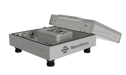
Nenocase
NNenoCase is an optional accessory for atomic force microscope LiteScope™;
NenoCase is a storage case enabling LiteScope to perform as a stand-alone device. It incorporates a passive anti-vibration system to ensure high-quality imaging outside the SEM chambers.
NenoCase can be purged with various gases used for measuring in different atmospheres.
NenoCase Key Features
Design
NenoCase has a compact platform made of aluminum alloy with appropriate adapters for the connection of LiteScope to the control electronics. Its base incorporates four separate components providing both vertical and horizontal vibration isolation. Lightweight materials are used. The transparent design of the cover enables the usage of optical and stereo microscopes when NenoCase is closed. It is possible to add custom feedthroughs.
Digital microscope specification
– Resolution 1.3 megapixels (1280×1024 pixels).
– Magnification up to 90×.
– Frame rate up to 30 fps (15 fps at 1.3 M).
– 8 white LED lights.
– Infrared cut-filter >650 nm.